|
|
|||||||||
|
Figures A to C (below) show various electron energy diagrams for two conducting specimens, 1 and 2.
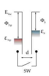 Figure A Electron energy level diagram for two conducting specimens, where  1
and 2
are the work functions of the materials, and 1
and 2
are the work functions of the materials, and
 1
and
2 represent their fermi levels. 1
and
2 represent their fermi levels.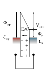 Figure B If an external electrical contact is made between the two electrodes their fermi levels equalise and the resulting flow of charge (in direction indicated) produces a potential gradient, termed the contact potential Vc, between the plates. The two surfaces become equally and oppositely charged. 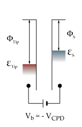 Figure C Inclusion of a variable "backing potential" Vb in the external circuit, permits biasing of one electrode with respect to the other. At the unique point where the (average) electric field between the plates vanishes, resulting in a null output signal. Theory Behind the Kelvin ProbeThe renowned Scottish physicist Sir William Thomson, later
Lord Kelvin showed over a century ago that a potential is generated between the
surfaces of two conductors when they are brought into electrical contact. This
contact potential depends on the work functions of the materials being used. The
work function is the amount of energy needed to release electrons from a
material's surface, and is related to the material's optical, electrical and
mechanical properties. When two materials with different work functions are
brought together, electrons in the material with the lower work function flow to
the one with the higher work function. If these materials are made into a
parallel plate capacitor, equal and opposite surface charges form. The voltage
developed over this capacitor is called the contact potential and measuring it
is done by applying an external backing potential to the capacitor until the
surface charges disappear, at that point the backing potential will equal the
contact potential.
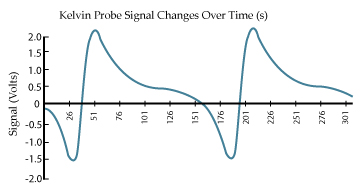
As the probe oscillates above the sample the voltage change is recorded. The peak-to-peak output voltage Vptp, is given by: Vptp = (Delta V - Vb)R.C0.w.e.sin(w.t + f) (Equation 2) Where Delta V represents the voltage difference between probe tip and sample, Vb is the externally applied emf used to balance (or null) the circuit, R is the I/V converter feedback resistance, C0 is the mean Kelvin Probe capacitance, Omega the angular frequency of vibration and Theta the phase angle. Epsilon is the modulation index (d1/d0) where d0 is the average distance between the sample and the probe tip and d1 is the amplitude of oscillation of the probe.
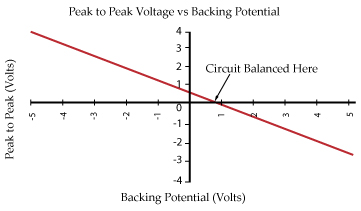
The backing potential Vb is set to a range of potentials and a plot of Vptp verses Vb is made. As can be seen from
Equation 2 this is a straight line. When Vptp = 0 the Work Function or Contact Potential of the surface is equal and opposite to Vb.
Traditional phase sensitive detection methods utilise a LIA (lock in amplifier) to detect the null output condition. However, these
systems have the disadvantage that at the balanced point, the signal to noise (S/N) ratio reaches a minimum, and noise creates an
offset voltage. A better method is to set Vb to a range of voltages and then extrapolate to the null signal condition, thus working
to a high S/N ratio. |
|
| KP Technology Ltd., Burn Street, Wick, Caithness, Scotland, KW1 5EH. Tel: + 44(0)1955 602777 | Contact |